Posts

Showing posts from 2007

nano radio

Image
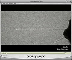
Nanotube radio on video The nanotube radio seen under a high-resolution transmission electron microscope, which allows researchers to observe the radio in action as it tunes in Derek & The Dominos playing Eric Clapton's "Layla." When not tuned in, the nanotube does not vibrate. As the researchers tune it to the proper frequency, however, the nanotube vibates at radio frequencies, which blurs its image. The nanotube is about 700 nanometers long and 10 nanometers in diameter — one ten-thousandth the width of a human hair. (Zettl Research Group/LBNL & UC Berkeley) View movie source: http://www.nanotech-now.com/news.cgi?story_id=26060 Also see : http://www.sfgate.com/cgi-bin/article.cgi?file=/c/a/2007/11/01/BUTBT44A2.DTL&type=business Physicists at UC Berkeley say they have produced the world's smallest radio out of a single carbon nanotube that is 10,000 times thinner than a human hair.

fab city updates : nov 07

Some recent news items on fab city and related semindia to apply for govt incentives within month Economic Times, India - Oct 10, 2007 "The company plans to invest USD $3 billion over the next five years at Fab City (an SEZ) near Hyderabad. We are in the process of applying for incentives ... semindia to export hardware to China Hindustan Times, India - Oct 11, 2007 So you thought India was for software and China was for hardware in making smart electronic devices? semindia, a non-resident Indian-led consortium that ... Embedded keen to start Hyd operations Business Standard, India - Oct 11, 2007 Another US-based company, Tessolve, is also in touch with the government to set up an assembly and testing plant in the Fab City . It has already announced ... Titan Energy to set up solar cell unit in Fab City Hindu, India - Oct 12, 2007 HYDERABAD: The Hyderabad-based solar photovoltaic module manufacturer, Titan Energy Systems, has announced plans to set up a 500 MW facility in t

haunting memories

http://www.nytimes.com/2007/09/11/technology/11storage.html?_r=1&th&emc=th&oref=slogin if an idea that Stuart S. P. Parkin is kicking around in an I.B.M. lab here is on the money, electronic devices could hold 10 to 100 times the data in the same amount of space. That means the iPod that today can hold up to 200 hours.... If he proves successful in his quest, he will create a “universal” computer memory, one that can potentially replace dynamic random access memory, or DRAM, and flash memory chips, and even make a “disk drive on a chip” possible....... His research group is able to slide the tiny magnets along notched nanowires at speeds greater than 100 meters a second. Since the tiny magnetic domains have to travel only submolecular distances, it is possible to read and write magnetic regions with different polarization as quickly as a single nanosecond — far faster than existing storage technologies.......

Kalam nanotech !

http://www.mbauniverse.com/innerPage.php?id=ne&pageId=316 When President Dr. A.P.J. Abdul Kalam visits West Bengal on a whirlwind tour on May 16 and 17, Indian Institute of Technology (IIT) campus at Kharagpur will be an important stop. At IIT-K, Dr Kalam will take two classes on Nano Technology for students of B. Tech., PG and Phd. at the Indian Institute of Technology (IIT) at Kharagpur on May 17. And here is the report after the event http://www.telegraphindia.com/1070518/asp/bengal/story_7794968.asp

nanodance

Image
found it !! see previous post (nanosnake) for details :-)

nanosnake

Image
just for fun... was helping out my labmate by taking some SEM pictures of his Bragg Gratings, when I just hit upon this one. Did not miss the chance.. Previously I also had a "dancing golden-X" picture, which was essentially a Ti-Au alignment pattern in the shape of a X which did not stick properly and got a li'l bent and was sticking up! Again, an SEM picture.. but can't find it now :-( .. had I been a blogger then, would have surely uploaded it here .... Is there any nano-photography competition ?! :-)

news from intel

"wafer packaging plant" ?! http://www.rediff.com/money/2007/apr/03intel.htm World's largest chip manufacturer, Intel Corporation on Tuesday said it awaits detailed guidelines of the semiconductor policy before deciding on setting up a manufacturing facility in India. "After the Cabinet approval, the government has notified the policy but we are waiting for the detailed policy guidelines before announcing any decision," Intel South Asia managing director Ramamurthy Sivakumar told PTI. The government in mid-March notified the semi-conductor policy with an expectation to attract Rs 24,000 crore (Rs 240 billion) of investment in the next three years. Intel, which is currently running a development centre in Bangalore, has been in constant dialogue with the Indian government for setting up a manufacturing base, most likely an assembly test manufacturing plant, commonly known as a wafer packaging plant. Intel has fifteen 12-inch wafer fabrication plants in the US, Ire

HSMC plans $4 bn chip plant in India

http://www.rediff.com/money/2007/mar/28chip.htm Hindustan Semiconductor Manufacturing Corporation on Wednesday announced a $4 billion investment plan for setting up a fab city in India in partnership with German technology major Infineon. HSMC would start the project with two foundries (fabrication plant) and would later scale it up to ten foundries, a company official said. The announcement comes less than a week after the government notified the semiconductor policy , which gives tax sops to companies setting up fab units. The semiconductors would be used in mobile phones, SIM cards, smart cards and automotive cards. The cost of each foundry will be $750-850 million for a 200 mm foundry, while it may cost up to $3.2-3.5 billion to set up a 300 mm foundry under the project. Phase one of the project will build nodes from 2009 onward under the 200 mm foundry, the official said. India's share in the global semiconductor market is negligible at present, but this project would enable t

10 billion ? really ?

http://www.rediff.com/money/2007/feb/23semi.htm Semiconductor policy aims at $10 billion investmentFebruary 23, 2007 01:09 ISTLast Updated: February 23, 2007 01:40 IST In a move that is perceived as a partial victory for the high-tech manufacturing sector in India and expected to attract investments of over $10 billion, besides generating employment, the Central government has announced a host of incentives in its much-awaited semiconductor policy, to buoy the semiconductor ecosystem. The government will bear 20 per cent of the capital expenditure in the first 10 years if a unit is located inside Special Economic Zones and 25 per cent in case of other units. The countervailing duty on capital goods would also be exempted in case of units outside SEZs. For semiconductor manufacturing (wafer fabs) plants, the threshold Net Present Value of investments would be Rs 2,500 crore and the NPV of investments for manufacturing other products would be Rs 1,000 crore. Assuming the projects have a

slowwwww.w..w..

http://pib.nic.in/release/release.asp?relid=23442 The Government is embarking on plans for launching a Nano Science and Technology Mission (Nano Mission) with estimated public investment of Rs. 1000 crore over the next five years to further intensify its promotional efforts in this area. As part of the Nano Mission it is planned to launch a variety of educational and HRD programmes, R&D programme, establish centers of excellence, promote institution-industry linked projects through increased public private partnerships, promoting entrepreneurship through establishment of business incubators, etc. The Nano Mission also plans to make special efforts for development and commercialization of nano technology, not only through public private partnerships but also by encouraging and enabling the private sector to invest in, and leverage, this sunrise technology.