Posts

is it for real ?

A post after such a long time... will it be the start of a restart or will it end up as an April fool joke... time alone will tell.. I need something to post, so let it be this news bit, http://www.fabtech.org/news/_a/intel_consolidates_its_lead_as_the_worlds_top_chipmaker/ (not just the intel part is interesting)

hopes fading ?

http://www.eetimes.com/news/semi/showArticle.jhtml?articleID=206900281 SemIndia's $3 billion fab project is likely to die a premature death as will another fab planned by India Electronics Manufacturing Corp. (IEMC). In addition, Korean investor June Min's plan to set up India's first fab in Hyderabad has been abandoned in favor of making photovoltaic products. India had made major strides in the last year, announcing a chip manufacturing policy. The incentive policy was intended to help launch state-of-the-art fabs here over the next few years. But the high expectations here for a domestic chip industry have faded as financial realities reemerge. Both SemIndia's fab, which would use technology from Advanced Micro Devices (AMD), and IEMC's fab appear to be dead in the water. ............... Despite the uncertainty, SemIndia's Systems unit is emerging as the company's flagship, and its manufacturing capability has bolstered the company's financial perfo...

some "nano-news"

http://blog.wired.com/wiredscience/2008/01/nanotech-used-2.html Damascus swords -- sharp enough to slice a falling piece of silk in half, strong enough to split stones without dulling -- owe their legendary qualities to carbon nanotubes, says chemist and Nobel laureate Robert Curl . The blades used so-called wootz steel, smelted with a technique developed 2000 years ago in India, where craftsmen added wood and other organic debris to their furnaces. The resulting carbon-laced steel, hard but flexible, was soon celebrated across the ancient world. -------------------------------------------------------------------------- http://www.cnet.com/matter-antimatter/8301-13641_1-9849464-44.html And now India proudly presented the spiritual successor to all of these -- the $2,500 Tata Nano , a "people's car" that is widely gushed about, not only for its surprisingly slick design but also for its innovations The Indian Economic Times even proclaims the " coming Nano Age :...

nano radio

Image
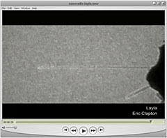
Nanotube radio on video The nanotube radio seen under a high-resolution transmission electron microscope, which allows researchers to observe the radio in action as it tunes in Derek & The Dominos playing Eric Clapton's "Layla." When not tuned in, the nanotube does not vibrate. As the researchers tune it to the proper frequency, however, the nanotube vibates at radio frequencies, which blurs its image. The nanotube is about 700 nanometers long and 10 nanometers in diameter — one ten-thousandth the width of a human hair. (Zettl Research Group/LBNL & UC Berkeley) View movie source: http://www.nanotech-now.com/news.cgi?story_id=26060 Also see : http://www.sfgate.com/cgi-bin/article.cgi?file=/c/a/2007/11/01/BUTBT44A2.DTL&type=business Physicists at UC Berkeley say they have produced the world's smallest radio out of a single carbon nanotube that is 10,000 times thinner than a human hair.

fab city updates : nov 07

Some recent news items on fab city and related semindia to apply for govt incentives within month Economic Times, India - Oct 10, 2007 "The company plans to invest USD $3 billion over the next five years at Fab City (an SEZ) near Hyderabad. We are in the process of applying for incentives ... semindia to export hardware to China Hindustan Times, India - Oct 11, 2007 So you thought India was for software and China was for hardware in making smart electronic devices? semindia, a non-resident Indian-led consortium that ... Embedded keen to start Hyd operations Business Standard, India - Oct 11, 2007 Another US-based company, Tessolve, is also in touch with the government to set up an assembly and testing plant in the Fab City . It has already announced ... Titan Energy to set up solar cell unit in Fab City Hindu, India - Oct 12, 2007 HYDERABAD: The Hyderabad-based solar photovoltaic module manufacturer, Titan Energy Systems, has announced plans to set up a 500 MW facility in t...
haunting memories

http://www.nytimes.com/2007/09/11/technology/11storage.html?_r=1&th&emc=th&oref=slogin if an idea that Stuart S. P. Parkin is kicking around in an I.B.M. lab here is on the money, electronic devices could hold 10 to 100 times the data in the same amount of space. That means the iPod that today can hold up to 200 hours.... If he proves successful in his quest, he will create a “universal” computer memory, one that can potentially replace dynamic random access memory, or DRAM, and flash memory chips, and even make a “disk drive on a chip” possible....... His research group is able to slide the tiny magnets along notched nanowires at speeds greater than 100 meters a second. Since the tiny magnetic domains have to travel only submolecular distances, it is possible to read and write magnetic regions with different polarization as quickly as a single nanosecond — far faster than existing storage technologies.......

Kalam nanotech !

http://www.mbauniverse.com/innerPage.php?id=ne&pageId=316 When President Dr. A.P.J. Abdul Kalam visits West Bengal on a whirlwind tour on May 16 and 17, Indian Institute of Technology (IIT) campus at Kharagpur will be an important stop. At IIT-K, Dr Kalam will take two classes on Nano Technology for students of B. Tech., PG and Phd. at the Indian Institute of Technology (IIT) at Kharagpur on May 17. And here is the report after the event http://www.telegraphindia.com/1070518/asp/bengal/story_7794968.asp

nanodance

Image
found it !! see previous post (nanosnake) for details :-)

nanosnake

Image
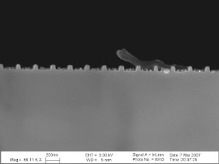
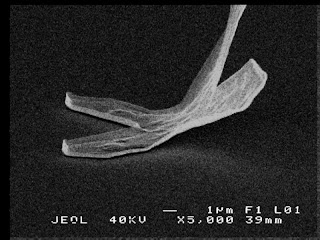
just for fun... was helping out my labmate by taking some SEM pictures of his Bragg Gratings, when I just hit upon this one. Did not miss the chance.. Previously I also had a "dancing golden-X" picture, which was essentially a Ti-Au alignment pattern in the shape of a X which did not stick properly and got a li'l bent and was sticking up! Again, an SEM picture.. but can't find it now :-( .. had I been a blogger then, would have surely uploaded it here .... Is there any nano-photography competition ?! :-)

news from intel

"wafer packaging plant" ?! http://www.rediff.com/money/2007/apr/03intel.htm World's largest chip manufacturer, Intel Corporation on Tuesday said it awaits detailed guidelines of the semiconductor policy before deciding on setting up a manufacturing facility in India. "After the Cabinet approval, the government has notified the policy but we are waiting for the detailed policy guidelines before announcing any decision," Intel South Asia managing director Ramamurthy Sivakumar told PTI. The government in mid-March notified the semi-conductor policy with an expectation to attract Rs 24,000 crore (Rs 240 billion) of investment in the next three years. Intel, which is currently running a development centre in Bangalore, has been in constant dialogue with the Indian government for setting up a manufacturing base, most likely an assembly test manufacturing plant, commonly known as a wafer packaging plant. Intel has fifteen 12-inch wafer fabrication plants in the US, Ire...

HSMC plans $4 bn chip plant in India

http://www.rediff.com/money/2007/mar/28chip.htm Hindustan Semiconductor Manufacturing Corporation on Wednesday announced a $4 billion investment plan for setting up a fab city in India in partnership with German technology major Infineon. HSMC would start the project with two foundries (fabrication plant) and would later scale it up to ten foundries, a company official said. The announcement comes less than a week after the government notified the semiconductor policy , which gives tax sops to companies setting up fab units. The semiconductors would be used in mobile phones, SIM cards, smart cards and automotive cards. The cost of each foundry will be $750-850 million for a 200 mm foundry, while it may cost up to $3.2-3.5 billion to set up a 300 mm foundry under the project. Phase one of the project will build nodes from 2009 onward under the 200 mm foundry, the official said. India's share in the global semiconductor market is negligible at present, but this project would enable t...

10 billion ? really ?

http://www.rediff.com/money/2007/feb/23semi.htm Semiconductor policy aims at $10 billion investmentFebruary 23, 2007 01:09 ISTLast Updated: February 23, 2007 01:40 IST In a move that is perceived as a partial victory for the high-tech manufacturing sector in India and expected to attract investments of over $10 billion, besides generating employment, the Central government has announced a host of incentives in its much-awaited semiconductor policy, to buoy the semiconductor ecosystem. The government will bear 20 per cent of the capital expenditure in the first 10 years if a unit is located inside Special Economic Zones and 25 per cent in case of other units. The countervailing duty on capital goods would also be exempted in case of units outside SEZs. For semiconductor manufacturing (wafer fabs) plants, the threshold Net Present Value of investments would be Rs 2,500 crore and the NPV of investments for manufacturing other products would be Rs 1,000 crore. Assuming the projects have a ...

slowwwww.w..w..

http://pib.nic.in/release/release.asp?relid=23442 The Government is embarking on plans for launching a Nano Science and Technology Mission (Nano Mission) with estimated public investment of Rs. 1000 crore over the next five years to further intensify its promotional efforts in this area. As part of the Nano Mission it is planned to launch a variety of educational and HRD programmes, R&D programme, establish centers of excellence, promote institution-industry linked projects through increased public private partnerships, promoting entrepreneurship through establishment of business incubators, etc. The Nano Mission also plans to make special efforts for development and commercialization of nano technology, not only through public private partnerships but also by encouraging and enabling the private sector to invest in, and leverage, this sunrise technology.

nice interview

Image
Nanotechnology is the new frontier of scientific research. President APJ Abdul Kalam is advocating new initiative on the research in the field of nanotechnology. As Prof. CNR Rao, chairman of the Scientific Advisory Committee to the Prime Minister, said recently: 'We missed the semiconductor revolution in the early 1950s. We had just gained independence. But with nanoscience and technology, we can certainly be on an equal footing with the rest of the world.' In its December 2006 issue, the Scientific American magazine published a list of 2006 Scientific American top 50 awards . The award lists the top 50 people in the field of research, business and policy making, who have influenced the world. Pulickel Madhavapanicker Ajayan, the Henri Burlage Professor of Engineering at Rensselaer Polytechnic Institute (Research) , Troy, New York, is among this list of top 50. He graduated in metallurgical engineering in 1985 from the Institute of Technology, Banaras Hindu University (IT-BHU)...

postponed... :-(

http://www.indianexpress.com/story/15323.html Chennai, October 24: Semindia Fab is postponing its proposed $3 billion investment to set up India's first chip manufacturing plant as it was unable to agree with the government on financial support to the unit's shareholding. Instead, it will set up a smaller facility for assembly, testing, manufacturing and packaging of memory chips (ATMC) next year, and review investment plans once a more favourable policy is announced by the Centre.

whats up with fab city ?

Uncertainties.... this sep 19 news tells us- be satisfied with the ATPM phase for now... hey, how many of that have we seen ?! http://www.dnaindia.com/report.asp?NewsID=1054040 And then, hopes back again, with this Oct 3 noose http://www.hindu.com/2006/10/04/stories/2006100411560100.htm Amidst accusations from, Oh well, the communists http://pd.cpim.org/2006/1022/10222006_ap.htm Me still have those fingers crossed....... and by the way, I heard a news (guess??) that AMD at present is busy figuring out if it wants to start a fab facility in NY (state) or not... and so isn't pushing as much for its India project... -------------------------------------------------- Meantime, if this is to be believed, good news on the "Universities catching up" front (hot news, just came out a few hrs before this posting) http://www.financialexpress.com/fe_full_story.php?content_id=144210 Europe’s largest independent research centre in nanotechnology and nanoelectronics is bullish on joint ...

QC and UFO

UFO applied in QC .... and no UFO is not "unidentifiable....." I mean ultrafastoptics http://www.sciencemag.org/cgi/content/full/313/5785/341 The fast dephasing of electron spins in an ensemble of quantum dots is detrimental for applications in quantum information processing. We show here that dephasing can be overcome by using a periodic train of light pulses to synchronize the phases of the precessing spins, and we demonstrate this effect in an ensemble of singly charged (In,Ga)As/GaAs quantum dots. This mode locking leads to constructive interference of contributions to Faraday rotation and presents potential applications based on robust quantum coherence within an ensemble of dots.

nanograss !!

Image
http://www.mphasetech.com/assets/images/nanograss10u.JPG nanotech batteries : http://www.mphasetech.com/html/nanotechnology.htm The image is a representative example of “nanograss” tubes. These tubes provide a “Superhydrophobic NanoStructured Surface” atop of which can be placed a droplet. The droplet sits above the tubes with little or no interaction with the tubes themselves. But by careful engineering the droplet can be made to fall within the space between the tubes encountering a greatly increased surface area and interacting with the tubes themselves to causing current to flow.. The drop can be engineered to occur upon a variety of stimuli: voltage, RF and/or others. Also see http://www.21stcentury.co.uk/technology/nanograss.asp

sc policy..

http://www.asianage.com/?sam=2:1:235:229571&headline=Semiconductor~policy~soon:~Maran Hyderabad, June 7: Union minister for communications and information technology, Dayanidhi Maran, said on Wednesday, that the government will be announcing its policy for the semiconductor industry in the next two weeks, even as work on India’s first semiconductor fabrication complex is expected to be launched later this month. SemIndia Fab, the company building the project, will begin the construction of a semiconductor testing and assembly unit, at an estimated cost of $100 million, Mr Vinod Agarwal, chairman and CEO of SemIndia Fab, said. The semiconductor complex is eventually estimated to cost $3 billion. ......... Mr Maran said the government was finalising the semiconductor policy keeping in mind that India could be the hub for the industry because of the increasing need for semiconductor chips in the domestic market. Asked whether the government would be investing in the equity of SemIndia...

nanotube brushes

Image
Source: Nature See the interesting news at http://starbulletin.com/2006/05/15/news/story06.html Pulickel Ajayan is of course quite a familiar name... looks like another Malayali is all set to make his mark.. or he has already ? Vinod P Vadakkeveedu - Guinness record holder for the smallest nanotube brushes Guess you can't just brush aside this one :-) . Quite an impressive record http://www2.hawaii.edu/~vinodpv/index.html So may be not only does nanoindia inc has a future, nanomalayali inc too... !!